In this 7th part of the Noise Toaster Lo-Fi Synth analysis, we’ll build the last two circuit sections and finish the PCB assembly. We started with the power supply and audio amplifier sections back in Part 2, and went on to build the VCO, LFO, ARG, and VCF circuits. We now turn our attention to the two last pieces of the puzzle ‒ the Voltage Controlled Amplifier (VCA) and the White Noise Source (WNS).
Noise Toaster VCA
Modulating the VCO has allowed us to control the pitch or frequency of our synth’s output. And modulating the VCF has allowed us to control tone or timbre. Now we add another circuit which lets us control the amplitude or loudness of the sound.
What is a VCA on a Synth?
A VCA or Voltage Controlled Amplifier is an amplifier circuit whose gain can be controlled by a control signal. VCAs are used to dynamically change the audio signal’s amplitude over time on a synthesizer.
How the Noise Toaster VCA Circuit Works
JFETs as Voltage Controlled Resistors
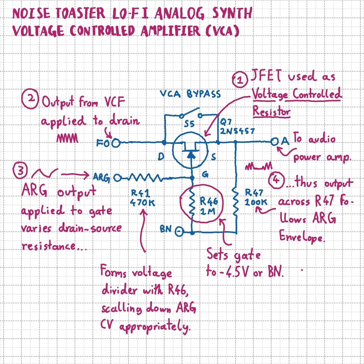
We saw in Part 6 that a JFET transistor can be used as a voltage-controlled resistor by biasing it below the “knee” of its operating parameters. Ray Wilson used this technique for the Noise Toaster’s VCF and VCA. Note that this simple circuit functions more like a voltage-controlled attenuator rather than a true voltage-controlled amplifier.
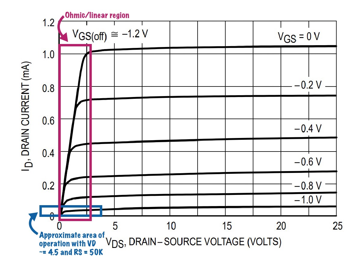
As seen in the 2N5457 Characteristics Curves (Figure 2), the relationship between drain-source voltage (VDS) and drain current, (Id) is more or less linear as long as VDS is below around 3.5V at VGS = 0. This is the Ohmic or linear area of JFET operation. The drain-source junction behaves as a resistance with the value:
Reqv = VDS/IDAs VGS goes more negative, the equivalent resistance is reduced. Thus, we can vary VGS to vary the drain-source junction’s equivalent resistance. Note that each VGS curve turns to the right and flattens out after a certain value of VDS is exceeded. This is known as the “pinch-off” point, above which the drain-source junction no longer behaves as a resistance. For correct voltage-controlled resistor operation without distortion, we need to make sure that VDS never raises beyond this point. However, as marked in Figure 2, the Noise Toaster’s VCA does leave the ohmic area at certain points. This introduces distortion to the signal. The JFET is not really deep into its linear region. This means that the circuit introduces a considerable amount of distortion.
Noise Toaster VCA Circuit Analysis
In the Noise Toaster VCA, JFET Q7 forms a voltage controlled attenuator along with R47. An envelope signal from the Noise Toaster’s ARG is applied to the JFET’s gate through R41. R46 and R41 form a voltage divider that scales down the input to the gate slightly. Since the ARG is DC coupled to R41, we can also think of R41 and R46 as providing a form of voltage-divider biasing.
The audio output from the Noise Toaster’s VCF is applied to the drain of Q7, and the attenuated signal appears at the JFET’s source across R47. The junction of Q7’s source and R47 is the input to the Noise Toaster’s audio amplifier. Closing switch S5 bypasses Q7 and applies the un-attenuated signal directly to the audio amplifier.
Noise Toaster ARG Output
The ARG output swings from around +3 to -3.5V around virtual ground. This is a swing from +1 to +7.5V relative to battery negative, centered around 4.25V.
Noise Toaster VCF Output
The VCF output swings about 4Vpp around virtual ground, this is a swing from +2.5 to +6.5V relative to battery negative, centered around 4.5V.
Noise Toaster VCF SPICE simulation
Modeling the ARG and VCF as DC voltage sources at their center voltages in SPICE gives us the following quiescent operating conditions:
Vd = 4.5V
Vg = 2.89V
Vs = 3.99V
VGS = -1.1V
VDS = 51mV
Id = 80uA
Thus, at the quiescent point, the equivalent drain-source resistance is:
RDS = 51mV / 80uA ~= 637.5 OhmsNoise Toaster VCF Load Lines

Since these values are far too low to visualize using the Datasheet graph. A more zoomed-in version of the 2N5457 characteristics curves generated using a SPICE simulation is presented in Figure 3. A load-line is the conventional way to visualize the operation of an amplifier. The left-most point on the vertical axis represents the theoretical maximum current flow, as determined by the circuit’s load resistance, in this case R47 in parallel with the audio amplifier’s input volume control potentiometer. Since both are R100Ks:
Id(max) = VD/Rs = VD/50000This gives us the following values for the maximum possible current flow for the low, mid, and high points of VD’s swing:
With VD = 6.5V, Id(max) = 6.5/50000 = 130uA
With VD = 4.5V, Id(max) = 4.6/50000 = 90uA
With VD = 2.5V, Id(max) = 2.5/50000 = 50uA
The rightmost point on the horizontal axis represents the highest possible drain-source voltage when the JFET is fully closed. The points at which the load line intersects with the various curves for each VGS indicate the corresponding value of VDS and Id which we can expect at that value of VGS. In figure 3, load lines are shown for VD = 6.5V, VD = 4.5V, and VD = 2.5V. With this graph, it is clear how the Noise Toaster’s VCA moves between the ohmic and pinched-off regions of operation to introduce asymmetrical distortion to the VCA output.
Noise Toaster VCA Distortion
Figures 4 and 5 show the result of this distortion assuming a pure sine-wave input for the minimum and maximum ARG output. Note that the Noise Toaster’s VCO cannot produce a pure sinewave. In reality, an already harmonically rich filtered square-wave or saw-tooth wave will be applied to the VCA through the VCF. The VCA’s asymmetrical clipping will further enhance the harmonic content. For more details, be sure to check out Ray Wilson’s own write-up on the MFOS website.
Another way to look at this circuit’s operation is an adjustable clipper, because it essentially never passes an unclipped signal. (Note that it IS possible for this circuit to pass a relatively “undistorted” waveform. This requires a very low input swing at the drain. A condition which is not met in the Noise Toaster) The SPICE simulation shows that adjusting the control voltage essentially control’s how much the top of the input signal is ” cut-off”.


Note that the above calculations and simulations may vary considerably from actual circuit operation due to the high variations in JFET characteristics. You may need to vary R47, R41, and R46 in order to obtained the desired results from the Noise Toaster VCA. There is bound to be discrepancy between the SPICE model used and an actual JFET as well. The above graphs and calculations are approximate and are only intended to help develop an intuitive understanding of the circuit functioning.
Noise Toaster VCA Gate Current
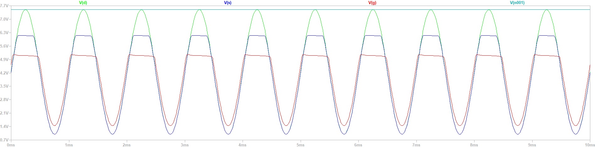
Another interesting quirk of the Noise Toaster VCA circuit is illustrated by the waveforms shown in Figure 6. The range of the VCF and ARG output swings cause VGS to swing to such an extent that the gate is allowed to go positive in relation to the source. This causes pulses of gate-current to flow that load down the voltage divider of R41 and R46. In a “low-fi” circuit such as the Noise Toaster, there is a lot of interaction between the various stages like this which keeps things musically interesting but difficult to electronically analyze.
Noise Toaster WNS
What is a White Noise Source on a Synth?
A WNS or White Noise Source is a circuit that generates random background noise or hiss. This atonal sound spans over the entire audio frequency spectrum and is usually used to add texture to a synth patch. White noise is also often used as the basis for creating various sounds such as percussion effects.
How the Noise Toaster WNS Circuit Works
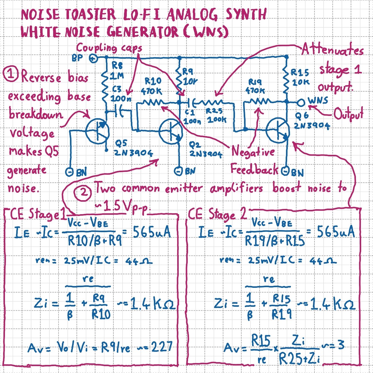
Bi-polar junction transistors (BJTs) produce random noise when their reverse bias base breakdown voltage is exceeded. The base-emitter junction of a transistor is essentially a diode – Ideally, a diode only allows the flow of electrons when it is forward biased. However, there is a limit it how much reverse bias the diode junction can withstand before it “breaks down” and starts conducting. This limit is specified as the diode’s breakdown voltage.
In the Noise Toaster’s WNS circuit (Figure 2), NPN transistor Q5’s emitter is tied to Battery Positive via R8, and its base tied directly to Battery Negative. This results in a heavy reverse bias across Q5’s base-emitter junction, causing a haphazard “noisy” current flow through the transistor. R8 protects Q5 from excessive current and also acts as a load resistance for the noise generated in the transistor.
Two Stage Amplifier using NPN Transistors
C3 couples the very low level white noise signal to a two stage amplifier made up of Q2, Q6, and their associated resistors. Both amplifier stages use a biasing arrangement called “collector-to-base feedback bias”, in which negative feedback is applied between the collector and base to stabilize the circuit. BJTs start to conduct more as they heat-up. As collector current rises, collector voltage decreases due the rising voltage drop over the collector load resistance (R9 for Q2 and R15 for Q6). Since the transistor’s base gets its bias from the collector, this results in a reduction of base current that compensates for the heating effect.
The voltage gain of this type of amplifier stage can be approximated by the following equation:
Av = RC/reWhere re, the equivalent emitter resistance is approximated by:
Re = 25mV/ICThe quiescent collector current IC can be found by:
IC ~= IE = (VCC-VBE)/(RF/β+RC)The input impedance is:
Zi = re / (1/β + RC/RF)Note that for Q2, RC is R9 and RF is R10. For Q6, RC is R15 and RF is R19. Solving the above equations give us the following results for each stage, assuming VBE = 0.7 and β = 100:
IE ~= IC = 565uA
Re = 44 Ohms
Zi = 1.5K Ohms
Av = 227
However, since first stage’s output is attenuated by a voltage divider formed by R25 and Q6’s input impedance, the actual gain of the second stage becomes:
Av = R15/re * Zi/R25+Zi = 3The total gain of both the stages is then:
Av1 * Av2 = 681The output of the WNS (after the two-stage amplifier discussed above) is around 1.5Vpp. This signal can be applied to the VCF by closing switch S4.
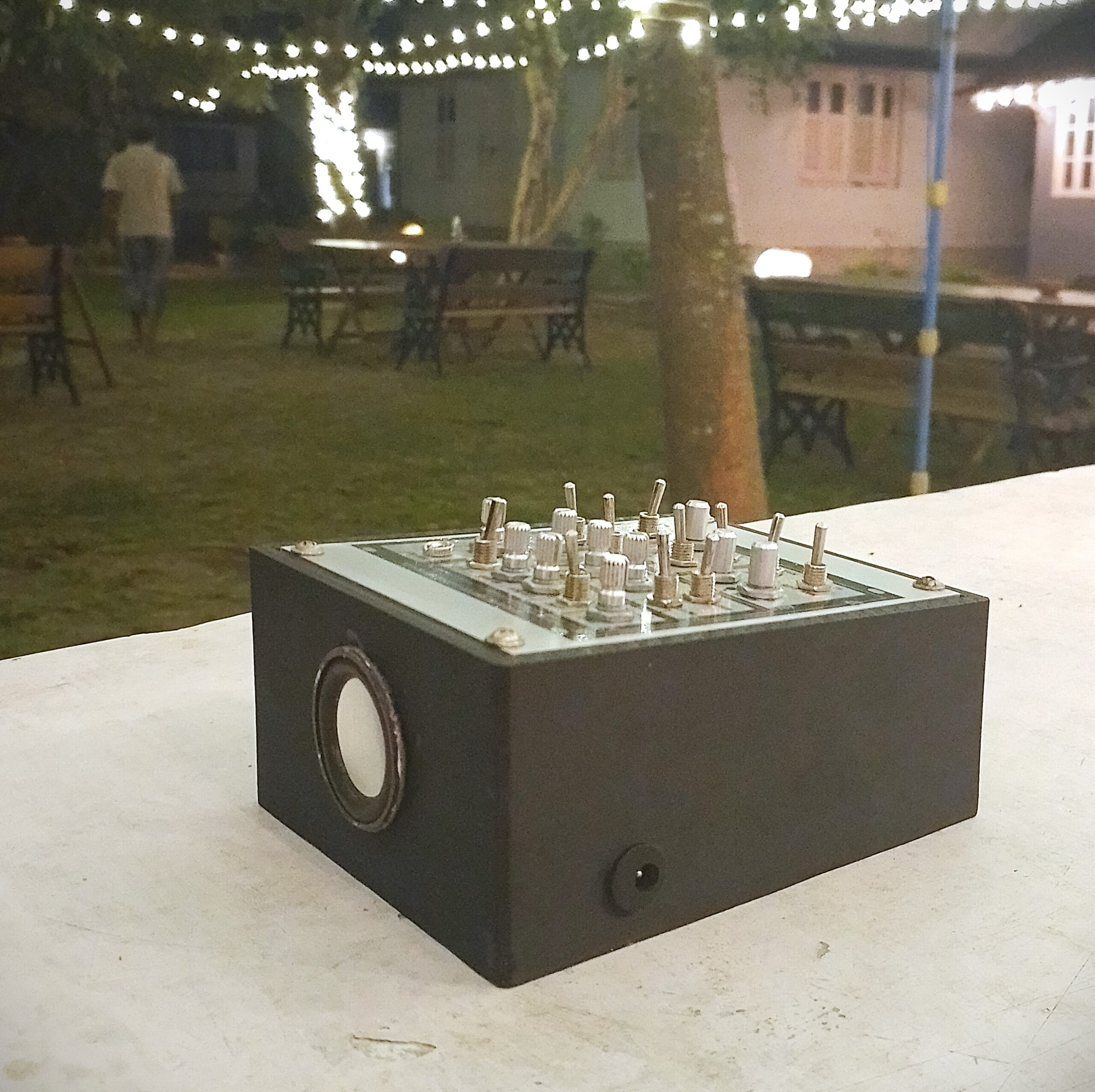
Building and Testing the Noise Toaster VCA and WNS
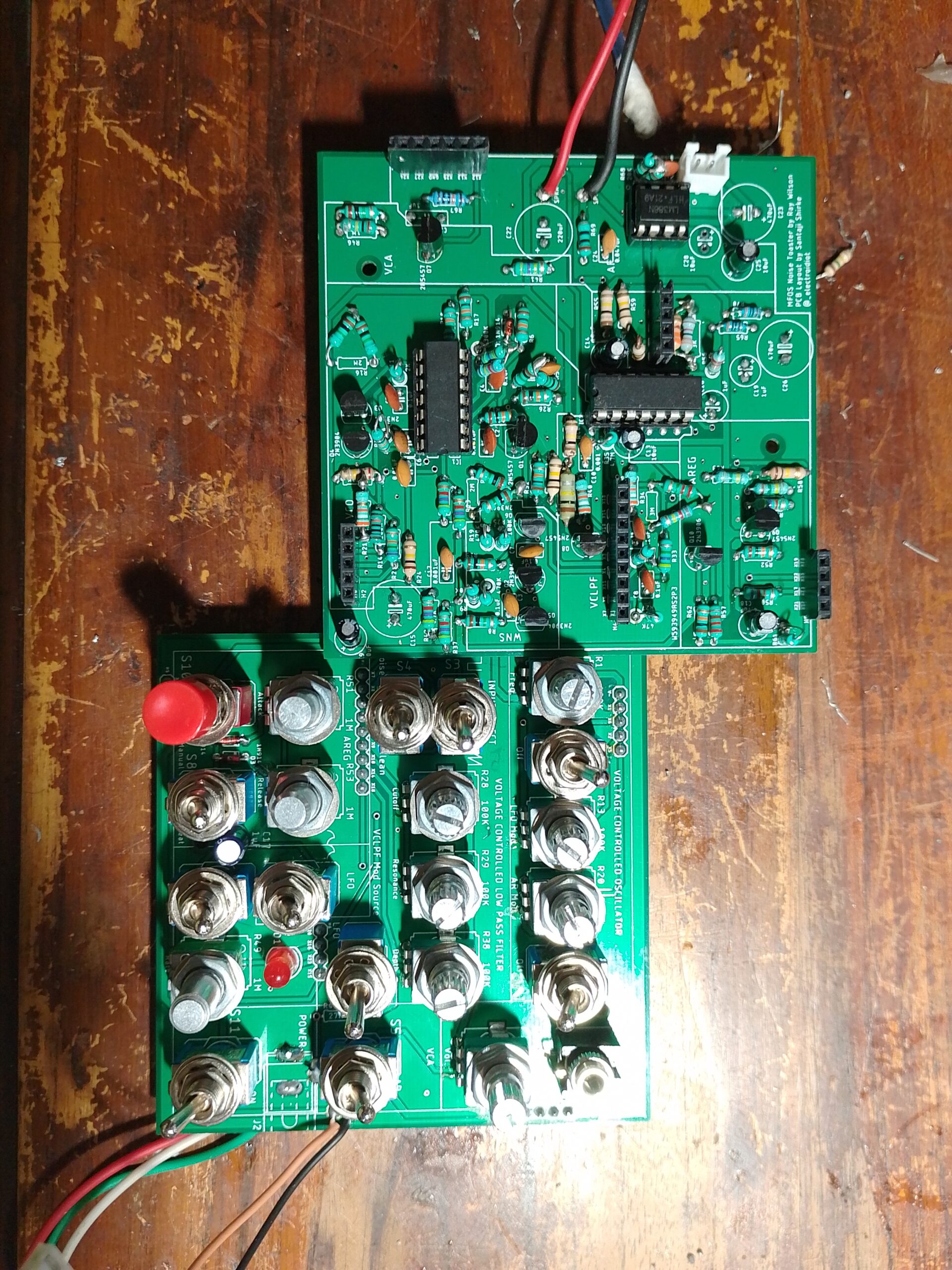
With the VCF and WNS assembled, the Noise Toaster’s circuit is complete and ready to generate some far-out alien-summoning sounds. To learn more about my experimental two-board sandwiched PCB design check out Part 1 of this series.
If you would like to build your own Noise Toaster, I recommend the official MFOS board or kit.

Build Your own Noise Toaster with Official MFOS PCBs and Kits…
3D Printed Synth Enclosure for the MFOS Noise Toaster
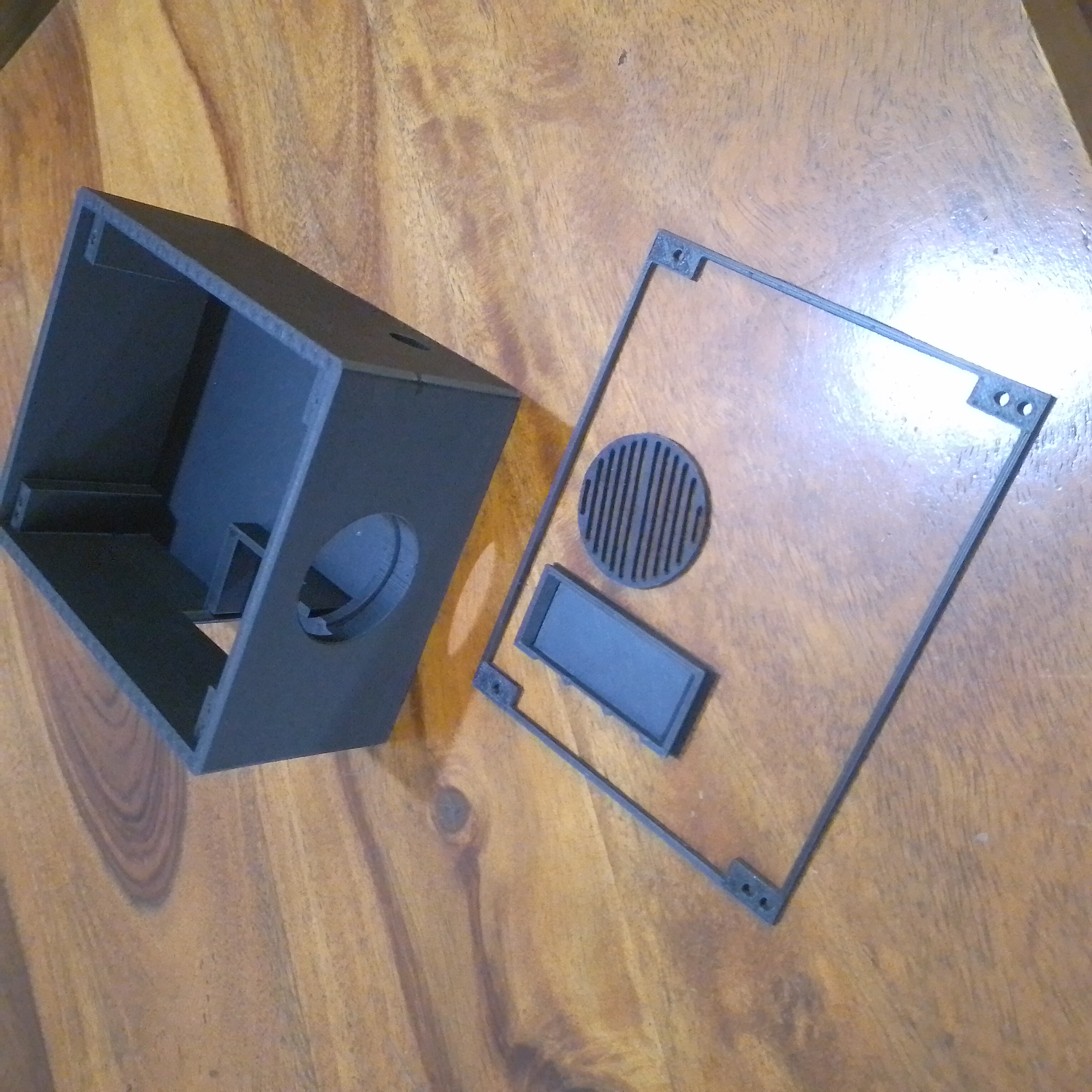

I had originally planned to make the enclosure as compact as possible, but after facing some clearance issues, I decided to make it Eurorack compatible instead. The redesigned enclosure takes Eurorack 20HP sized front panels. The compact size of my two-board design leaves enough room on the front for additional inputs or controls for future circuit modifications. The snap-fit battery cover from the original design is retained, however the snap-fit speaker grill was discarded for this iteration of the build due to clearance issues.
Noise Toaster Synth Mods
Ray Wilson designed to Noise Toaster to be easily hackable and expandable. There are some suggested circuit mods on the official Music from Outer Space website as well as various other sources. A particularly cool build is this fully patchable Noise Toaster by Kurt James Werner. I do plan to try out some of these modifications in the future, so be sure to subscribe to the _electrodiot newsletter below to stay updated!
Get Notified of New Posts, subscribe to the _electroidiot Mailing List.
Recommended Reading
Learn More About Synth Basics with Ray Wilson’s Excellent Book

Make: Analog Synthesizers. A Modern Approach to Old-School Sound Synthesis by Ray Wilson.
Check out following resources to learn more about the MFOS Noise Toaster:
- Make: Analog Synthesizers by Ray Wilson.
- Official Noise Toaster page on the Music from Outer Space website.
- 2N5457 JFET datasheet by Motorola.
- “A guide to using FETs for voltage controlled circuits, Part 1” article EDN by Ron Quan.
- CCRMA – MFOS Noise Toaster mod (stanford.edu) article by Kurt James Werner
Other Posts in this Series
- Noise Toaster Lo-Fi Synth Build and Analysis: Part 1 – Introduction
- Noise Toaster Lo-Fi Synth Build and Analysis: Part 2 – Power Supply and Audio Power Amplifier
- Noise Toaster Lo-Fi Synth Build and Analysis: Part 3 – CV Mixer, Expo. Converter, and VCO
- Noise Toaster Lo-Fi Synth Build and Analysis: Part 4 – Low Frequency Oscillator (LFO) Circuit Analysis
- Noise Toaster Lo-Fi Synth Build and Analysis: Part 5 – Attack Release Envelope Generator
Join the Conversation
If you notice any mistakes or errors, please feel free to let me know in the comments below.


Leave a Reply