Adding an LFO to modulate our VCO‘s frequency has already made our synth much more interesting. Let’s step things up a notch by adding another CV source – an AREG or Attack Release Envelope Generator.
This is part 5 of a multi-part series about the MFOS Noise Toaster Lo-Fi Analog Synthesizer. Make sure to check out the previous installments to fully understand how the Noise Toaster’s circuits work together.
In this article, we will learn about the Noise Toaster AREG circuit. Let’s see how it works and what we can do with it.
What is an AREG in a Synth?
An AREG or Attack Release Envelope Generator is a circuit that creates a varying control voltage or “envelope” to modulate another signal. The AREG’s output has a distinct “attack” portion in which its voltage rises to its peak level. This is followed by a release section in which the output falls back to 0. An AREG gives you a lot of control over the sound of your synthesizer with independently adjustable attack and decay times.
Attack, Decay, Sustain, and Release.
More sophisticated envelope generators also allow control over decay. Decay is the time required for the waveform to “settle” from its attack peak to a steady level. How long the waveform stays at this level before the release section starts is known as sustain.
As Ray Wilson of MFOS designed the Noise Toaster to be simple and “Lo-Fi”, its envelope generator does not feature adjustable decay or sustain.
How the Noise Toaster AREG Circuit Works
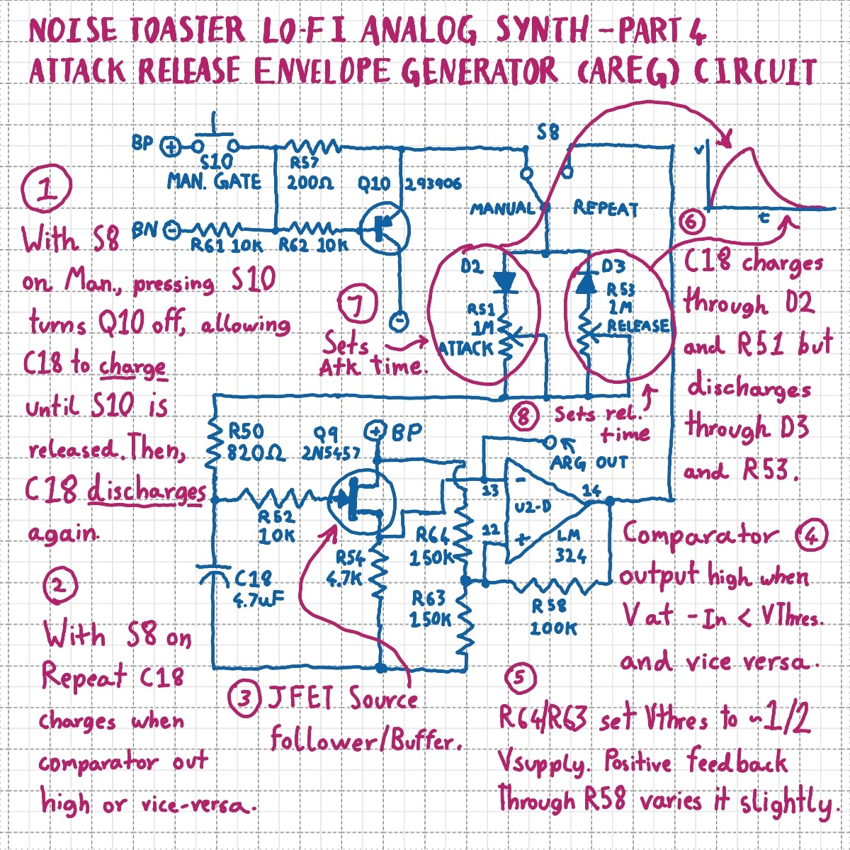
The Noise Toaster AREG circuit has two modes of operation: repeat and manual. In repeat mode, the circuit acts like an oscillator outputting a continuous waveform. In manual mode, closing a switch triggers the attack section of the envelope. The output then sustains for as long as the switch is closed. Leaving the switch triggers the release section of the envelope and the output dies out until manually triggered again.
Independently Controlling Attack and Release
When we looked at the VCO and LFO circuit, we saw how an RC circuit’s time constant can be used to set an oscillator’s frequency. The Noise Toaster AREG’s output is essentially a buffered version of the voltage across a capacitor.
Referring to Figure 1, we can see that a pair of diodes (D2 and D3) are used to control the flow of timing capacitor C18’s charging and discharging current. Note that the anode of D2 and the cathode of D3 are tied together. As you may know, an ideal diode only conducts when its anode is positive in relation to its cathode. In the Noise Toaster AREG circuit, C18 charges via D2, attack time control potentiometer R51, and current limiting resistor R50 when a positive voltage is applied at the junction of the two diodes. When a negative voltage is applied at this point, C18 will discharge through R50, release time control potentiometer R53 and diode D3. In this way, we can Independently adjust C18’s charge and discharge times.
JFET Buffer
The voltage across the capacitor is fed to JFET Q9’s gate pin and the output is taken from its source pin. The high input impedance at Q9’s gate prevents output current draw from affecting C18’s charge and discharge time. This amplifier circuit configuration is known as a source-follower. Although there is no voltage gain, the circuit provides current gain for impedance matching.
Manually Triggering the AREG
When AREG mode switch S8 is set to the manual position, the voltage at the junction of D2 and D3 is held at battery negative or BN by PNP transistor switch Q10. Pressing momentary switch S10 applies battery positive (BP) to Q10’s base, biasing the transistor off. Now, the junction of D2 and D3 is no longer forced negative through Q10. As a result, C18 charges through forward biased diode D2, attack time pot R51, and R50. The voltage across C18 climbs at a rate determined by the setting of R51. This creates the rising or “attack” part of the envelope.
Once C18 is fully charged, the output stays constant until S10 is released. Releasing S10 turns Q10 on again, forcing the junction of D2 and D3 negative. Now D2 is reversed biased and D3 is forward biased. This results in C18 discharging through R50, release time setting pot R53, and D3. R53’s setting determines how long C18 takes to discharge. This creates the falling or “release” part of the envelope.
Once C18 is discharged, the output stays dormant until S10 is pressed again.
Repeating AR Envelope
When S8 is set to repeat, the AREG acts as a low-frequency oscillator. The output wave-form of which can be shaped by adjusting the attack and release controls. In repeat mode, the junction of D2 and D3 is tied to the output of op-amp comparator U2-D.
R63 and R64 set the comparator’s threshold voltage to around half the supply voltage, and positive feedback from R58 adjusts this based on the op-amp’s output. The comparator’s – input is tied to Q9’s source which follows the voltage across C18. Thus, U2-D’s output saturates high when the voltage across C18 is below the threshold voltage. This in turn allows C18 to charge through D2, attack time pot R51, and R50.
When the voltage across C18 climbs to above the threshold voltage, U1-D’s output jumps low again. Now C18 starts to discharge through R50, R53, and D3 until the voltage across it drops to below the threshold voltage. This again puts U1-D in high saturation and the cycle repeats.
Learn More About Synth Basics with Ray Wilson’s Excellent Book

Make: Analog Synthesizers. A Modern Approach to Old-School Sound Synthesis by Ray Wilson.
If you would like to learn more about the Noise Toaster and synth DIY, I highly recommended Ray Wilson’s book “Make: Analog Synthesizers”. Wilson introduces some basic analog synthesizer concepts and explains the Noise Toaster circuit in his own words (he designed it!). There is also some great stuff on op-amp basics and common op-amp circuits for synth DIY.
Building and Testing the Noise Toaster’s AREG
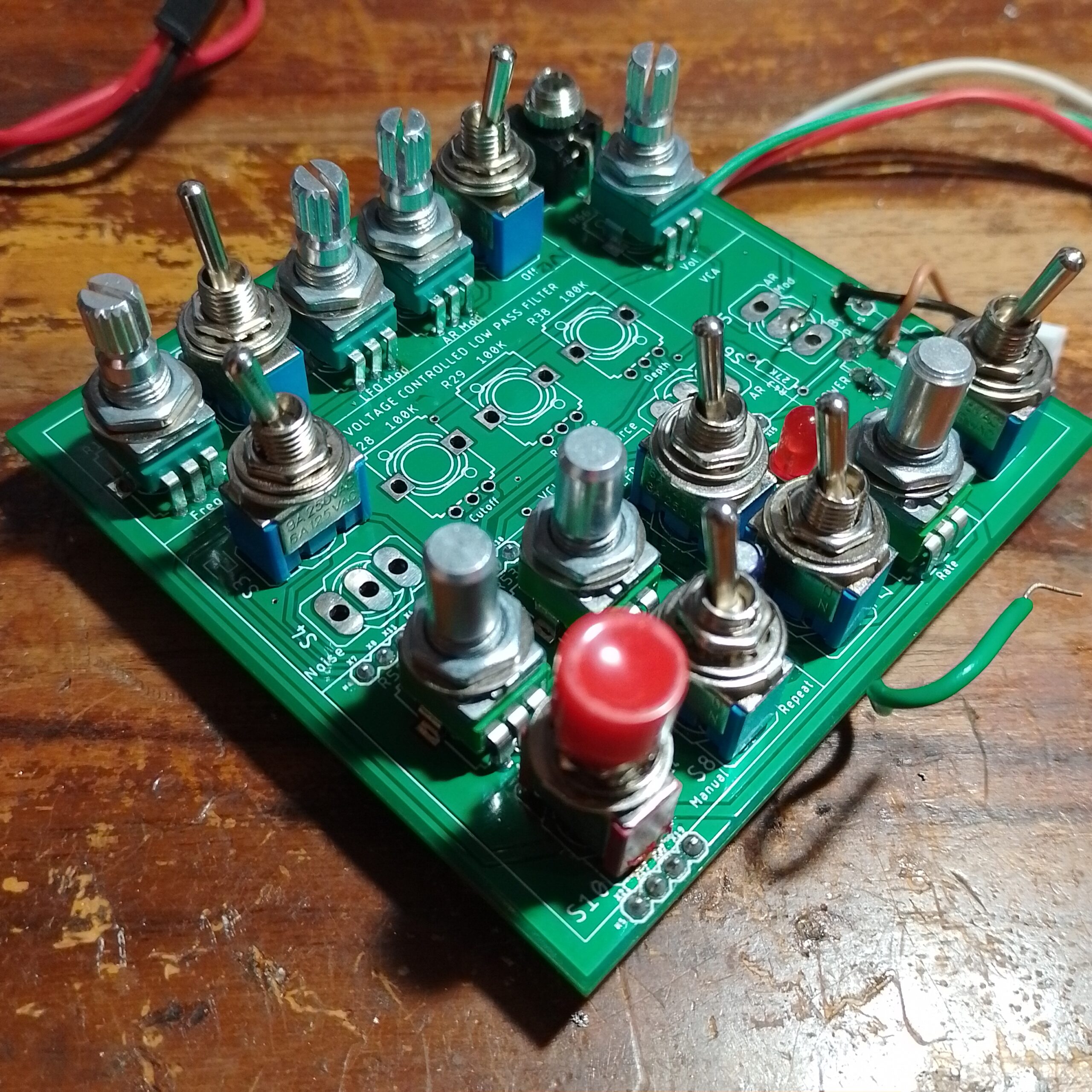
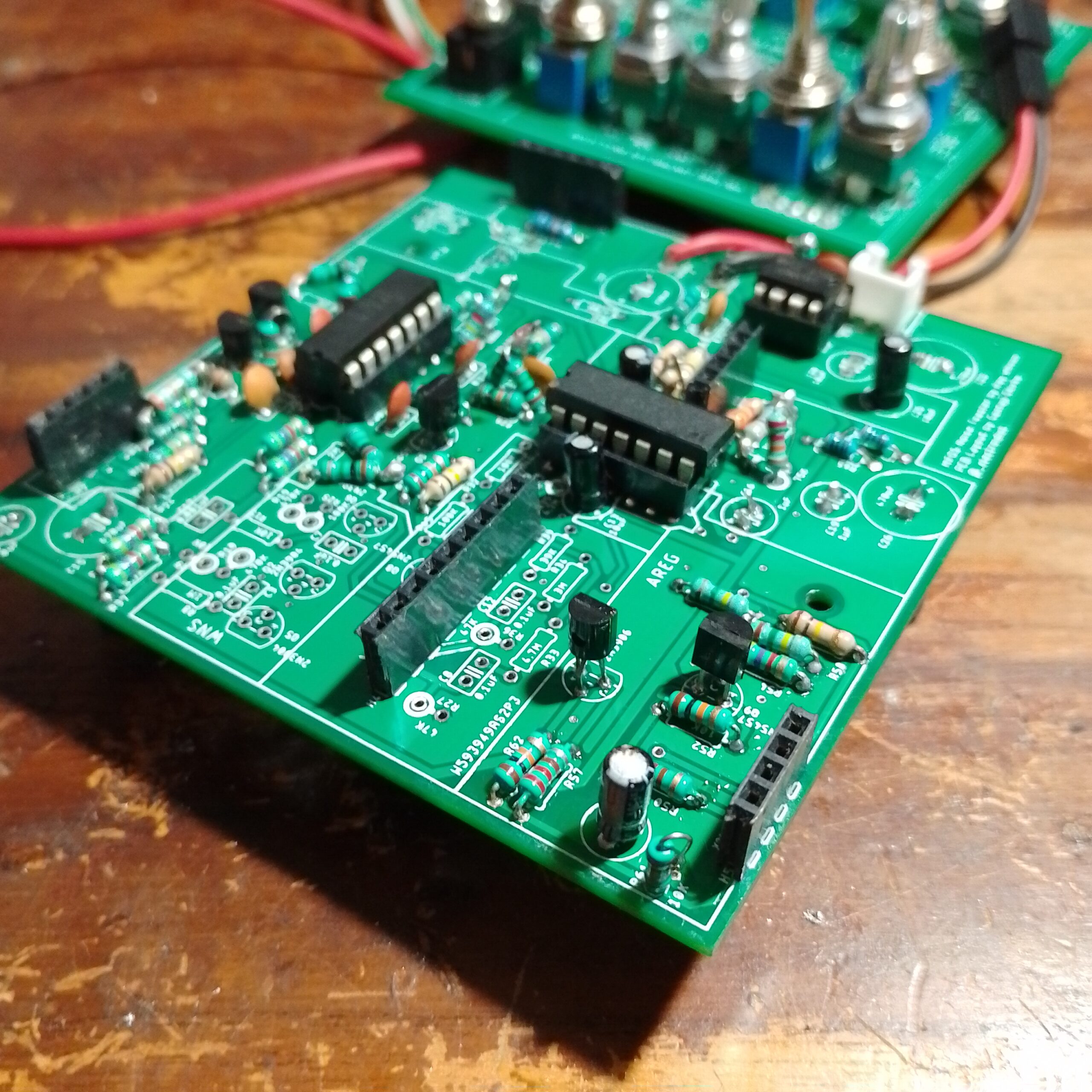
With the AREG section assembled, we now have two ways to modulate the VCO’s frequency. We can have the LFO and AREG modulating the VCO at the same time or turn down the mod depth control of either. You will find that the ability to adjust the attack and release time of the modulating envelope really opens up some fun new noise making possibilities. To learn more about my experimental sandwiched construction PCB design for the Noise Toaster, refer back to Part 1 of the series. If you would like to build your own Noise Toaster, I suggest you get an official MFOS board or kit.

Build Your own Noise Toaster with Official MFOS PCBs and Kits…
Both the LFO and AREG can do more than just modulate the VCO frequency. In the next part, we will build and analyze the voltage-controlled filter – another essential analog synthesizer circuit that will allow us to mess with the tonal character of the VCO output using either the LFO or AREG as a control signal.
Follow @_electroidiot on Instagram to stay updated and subscribe to the _electroidiot mailing list below to get notified of new posts!
Get Notified of New Posts, subscribe to the _electroidiot Mailing List.
Recommended Reading
Check out following resources to learn more about the MFOS Noise Toaster:
- Make: Analog Synthesizers by Ray Wilson.
- Official Noise Toaster page on the Music from Outer Space website.
Other Posts in this Series
- Noise Toaster Lo-Fi Synth Build and Analysis: Part 1 – Introduction
- Noise Toaster Lo-Fi Synth Build and Analysis: Part 2 – Power Supply and Audio Power Amplifier
- Noise Toaster Lo-Fi Synth Build and Analysis: Part 3 – CV Mixer, Expo. Converter, and VCO
- Noise Toaster Lo-Fi Synth Build and Analysis: Part 4 – Low Frequency Oscillator (LFO) Circuit Analysis
- Noise Toaster Lo-Fi Synth Build and Analysis: Part 5 – Attack Release Envelope Generator
Join the Conversation
If you notice any mistakes or errors, please feel free to let me know in the comments below.


Leave a Reply