The Noise Toaster is built around a ramp core analog oscillator which acts as the synth’s main signal source. The frequency can be modulated by control voltages from various sources – this makes it a Voltage Controlled Oscillator (VCO).
In this article, we take an in-depth look at how the Noise Toaster’s VCO circuit functions.
How the Noise Toaster Lo-Fi Synth’s VCO Works
What are Voltage Controlled Oscillators in Synthesizers?
Voltage Controlled Oscillators used in synthesizers usually change their output pitch exponentially with a linear change in input voltage. This is because the difference in frequency between musical notes or pitches follows an exponential relationship. The Noise Toaster’s VCO can be controlled by 3 internal CV Sources:
- The base frequency setting potentiometer (R1 in Figure 1).
- The Low Frequency Oscillator (LFO).
- The Attack Release Envelope Generator (AREG).
The freq. potentiometer outputs a static CV, while the LFO and AREG CVs change dynamically. We will learn about the latter two sections later in this series.
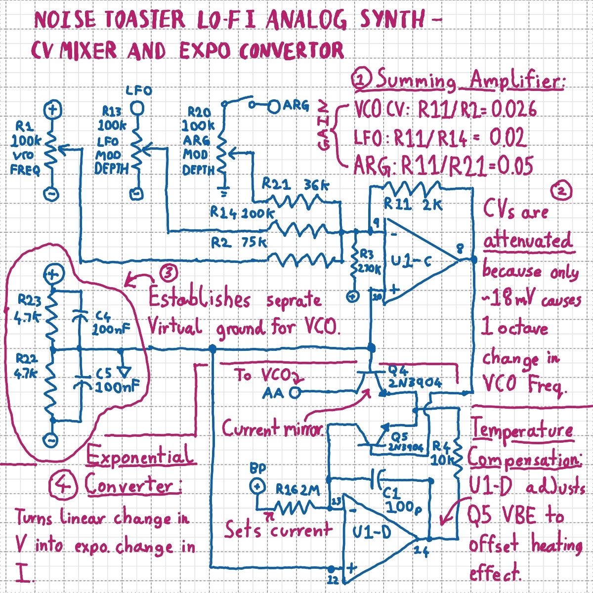
Summing Amplifier
The CV inputs to the VCO section are combined, buffered, and attenuated by the Inverting Summing Amplifier formed by U1-C. The gain for each input is set by the relationship of feedback resistor R11, and each corresponding input resistor (R2, R14, and R21 for Freq. Control, LFO, and AREG respectively). The LFO and AREG outputs can be attenuated by their corresponding mod depth potentiometers before being applied to the input.
Estimating the Gain and Output Voltage
The gain is less than unity. This is because the exponential converter only needs around 18mV of voltage change to change pitch by 1 octave. Gain for each individual input can be calculated as follows:
Av VCO CV = -R11/R2= -2000/75000 = -0.026
Av LFO= -R11/R14= -2000/100000 = -0.02
Av ARG= -R11/R21 = -2000/36000= -0.05
Thus, the input voltages needed for an 18mV output change from each input, after the corresponding potentiometer are:
| Input | Voltage |
| VCO CV (Freq. Control) | 0.69V |
| LFO | 0.9V |
| AREG | 0.36V |
Note that 270K resistor R3 tied to battery positive (BP) also affects the summing amplifier’s output. Ignoring the LFO and AREG Inputs, we can estimate U1-C’s Vout when R1 is set to its mid-point as:
Vout = ( −VR2∗(R11/R2) ) + ( −VR3∗(R11/R3) ) = −0.15VExponential Converter
This stage converts the linear voltage change at the summing amplifier’s output into an exponential current change. This current is the input to the VCO’s core. In Figure 1, I have redrawn this section to make it easier to understand.
Voltage-Current Relationship in BJTs and the Effect of Temperature
The collector-emitter current (IC) of a Bi-Polar Junction Transistor (BJT) is an exponential function of its base-emitter voltage (VBE). This is exactly what we need for an exponential converter.
Unfortunately, IC and VBE are also heavily affected by the transistor’s temperature. Thus, we need a way to compensate for this or our VCO will be extremely unstable. One way is using another nearby transistor to track VBE, then invert and use this to offset the increasing IC.
Temperature Compensation Using an Op-Amp Current Source
In the Noise Toaster, op-amp U1-D is set up as a current source with Q5 in its feedback loop. You may be familiar with the golden rules of op-amp circuit analysis:
- The op-amp tries to maintain the inputs at the same potential.
- the inputs draw no current.
Thus, since the + input is at circuit ground, the voltage drop over current setting resistor R16 will be 4.5V. Since this current can’t flow into the input, it flows in the feedback loop in which our “load” is placed. The load current will be:
4.5/2000000 = 2.25uAAs Q5 heats up it tries to draw more current. This is countered by the op-amp changing its output in reaction. As current tries to increase, U1-D increases its output, reducing the voltage dropped over R4 and Q5’s VBE. Note that Q5’s base is somewhere near virtual ground, and U1-D’s output is negative in relation to this! Essentially, VBE is reduced by the exact amount needed to counter the change in transistor parameters trying to increase IC.
Q4’s collector is connected to the VCO core’s input. Its VBE junction is connected across that of Q5. Thus, both transistors are forced to have the same quiescent current (Since Q4 and Q5 are mounted close together, it is assumed that both exhibit a similar heating effect).
Q5’s base is connected to the summing amplifier’s output, so its VBE depends on the outputs of both op-amps. Its IC however is purely set by U1-D.
As Q4 is not in the feedback loop, IC is determined by its VBE. This is indirectly determined by the summing amplifier output while also being “temperature compensated” by Q5!
How the Noise Toaster’s VCO Works
The exponentially changing current being “sunk” by Q4 sets the VCO core’s frequency here’s how it works:
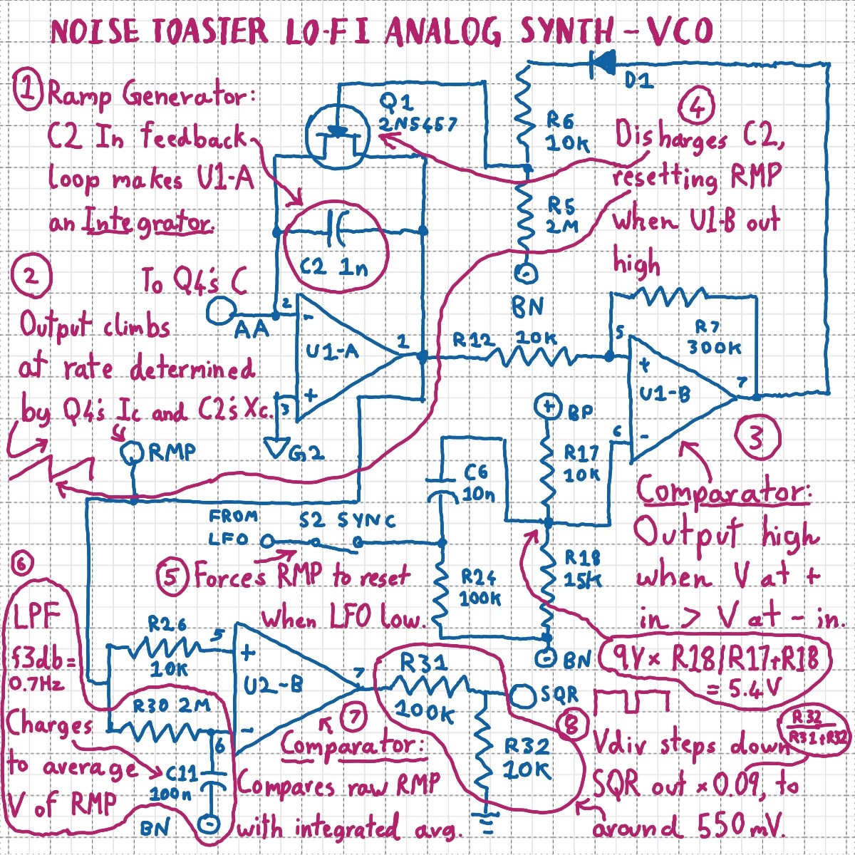
Noise Toaster Ramp Core
Referring to Figure 2, U1-A is set up as an integrator with its – input connected to the Q4 current sink. The amount of current sunk by Q4 determines how long C2 takes to charge. As C2 charges, the voltage at U1-A’s output ramps up towards battery positive. The ramp output is taken from this point; however, we need the ramp to “reset” at a certain voltage level. Otherwise, the output will simply climb until U1-A saturates and stay there. To accomplish this, a non-inverting comparator U1-B is connected to U1-A’s output. Its threshold is set by R17 and R18 to around 5.4V. (This value changes slightly depending on the comparator’s output due to “hysteresis” provided by positive feedback resistor R7)
Resetting the Sawtooth Core with a JFET Switch
When the input exceeds this threshold voltage, U1-B’s output goes high, turning on JFET switch Q1. When Q1 turns on, C2 is shorted, causing U1-A’s output to instantly fall to 0. This makes the comparator output go low as well, turning off Q1. C2 can now begin charging again, causing the cycle to repeat. The LFO output can be connected to the comparator’s threshold voltage divider via S2, the sync switch. This will force the comparator to go low whenever the LFO output drops, thus “syncing” the two oscillators.
Noise Toaster Square-Wave Output
The ramp core’s output is a fed to another comparator formed by U2-B. Here, the threshold voltage is set by an integrator or low-pass filter formed by R30 and C11. C11 charges to the “average” value of the ramp, so U2-B’s output goes high whenever the actual waveform exceeds this. U2-B thus outputs a square-wave as it switches states. Since this is a rail-to-rail output, voltage divider R31/R32 steps down the voltage to around 550mV at the square-wave output.
In addition to the above summary, you may have also noticed the voltage divider of R23/R22. This establishes a separate virtual ground for the VCO section to avoid unwanted interaction with the other circuits. To learn more about the Noise Toaster, check out the MFOS Website and Ray Wilson’s book “Make: Analog Synthesizers”.
Building and Testing the Noise Toaster’s VCO
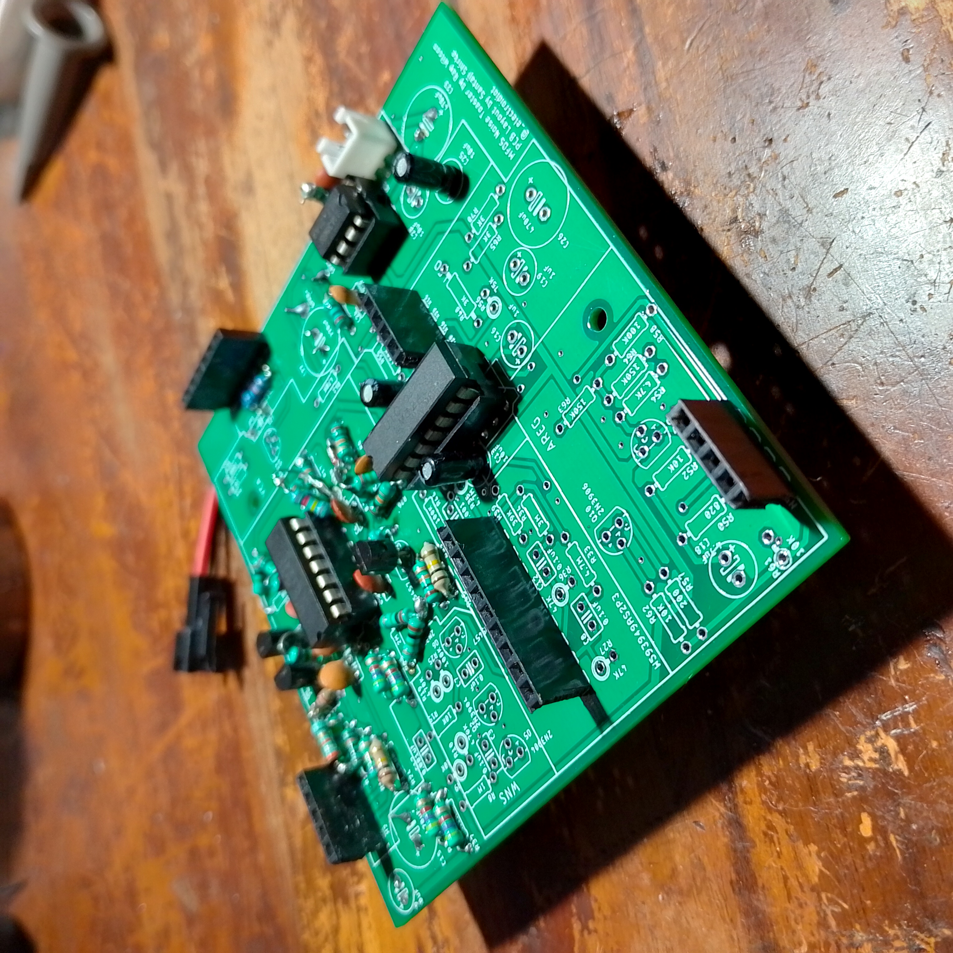

Now that we have a signal source, we can finally hear some sounds out of our synth. The VCO output normally passes through the VCF and VCA, but for testing, I shorted it to the volume control. To learn more about the PCB design, refer back to Part 1 of this series.
In the next part of this series, we will build the LFO and have fun with dynamically modulating the VCO. Follow @_electroidiot on the ‘gram to stay updated and subscribe to the _electroidiot mailing list to stay updated!
Get Notified of New Posts, subscribe to the _electroidiot Mailing List.
Recommended Reading
Check out following resources to learn more about the MFOS Noise Toaster:
- Make: Analog Synthesizers by Ray Wilson.
- Official Noise Toaster page on the Music from Outer Space website.
- Exponential converters and how they work article by North Coast Synthesis Ltd.
- A tutorial on exponential convertors and temperature compensation article by René Schmitz
- DIY VCO Part 2: The simplest exponential converter video by Moritz Klein
- Learning the Art of Electronics, a Hands-On Lab Course by Thomas C. Hayes, particularly chapters 5 and 6 on transistor behavior and op-amp basics respectively.
Other Posts in this Series
- Noise Toaster Lo-Fi Synth Build and Analysis: Part 1 – Introduction
- Noise Toaster Lo-Fi Synth Build and Analysis: Part 2 – Power Supply and Audio Power Amplifier
- Noise Toaster Lo-Fi Synth Build and Analysis: Part 3 – CV Mixer, Expo. Converter, and VCO
- Noise Toaster Lo-Fi Synth Build and Analysis: Part 4 – Low Frequency Oscillator (LFO) Circuit Analysis
- Noise Toaster Lo-Fi Synth Build and Analysis: Part 5 – Attack Release Envelope Generator
Join the Conversation
If you notice any mistakes or errors, please feel free to let me know in the comments below.


Leave a Reply