Getting Started with the 555 Timer – Everything You Need to Know
The 555 Timer is one of the most popular integrated circuits of all time. Its versatility has made it a favourite among hobbyists, who keep discovering creative uses for the chip beyond its original purpose. No matter where your interests lie in the vast field of electronics, you will almost certainly need to use one at some point! This article will introduce the 555 timer and explain its functioning and basic circuit configurations with a focus on building an intuitive understanding of how it works. Learning about the 555 Timer also introduces you to some important electronics concepts and will help you develop your understanding about electronics systems.
What is the 555 Timer?
The 555 is a timer and oscillator integrated circuit that was designed in the early 1970s by engineer Hans Camenzind. By using an external timing capacitor and resistor network, the 555 timer can be configured as a very stable pulse generator or oscillator. It was one of the first general purpose, commercially marketed ICs. Over 40 years later, it remains hugely popular and has been used in everything from toys to spacecraft.
There are various versions of the chip, but this post will focus on the original TTL version, which is usually labelled as NE555, NA555, or SE555.
555 Timer IC Pinout
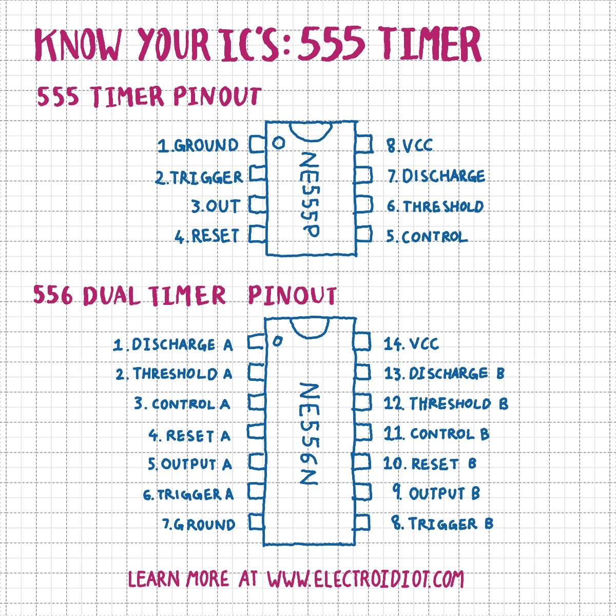
The 555 timer is available in various packages, the most common being the 8-pin PDIP (through-hole) and SOIC(SMD) versions. There is also a 14-pin dual timer package called the 556, which contains two separate 555 Timers in one chip. The pinouts for both types are shown in Figure 1 above.
Let’s start by taking a quick look at the chip’s pin-out, and briefly describing each pin’s function. Note that the pin numbers in this article correspond to the single 555 Timer 8-pin package as shown in Figure 1.
555 Timer Pin Functions
The 555 timer’s pins and their basic function are as follows:
PIN 1 – GROUND: The main ground reference for the chip.
PIN 2 – TRIGGER: Taking it under 1/3rd of VCC sets output (pin 3) high and discharge (pin 7) open.
PIN 3 – OUTPUT: The output will be high (around VCC-2) or low (slightly above ground) depending on the voltages on pins 3, 5, and 6.
PIN 4 – RESET: Taking it low when the timer is on forces the output and discharge pins to go low.
PIN 5 – CONTROL: Can be used to alter the threshold voltage (see pin 6) for modulation purposes. If unused, it should be tied to ground via a 10nF capacitor.
PIN 6 – THRESHOLD: Usually connected to a timing capacitor. When it is taken to over 2/3rds of VCC, it takes the output and discharge pins low.
PIN 7 – DISCHARGE: Shorts to ground when output goes low. Used for discharging timing capacitor.
PIN 8 – VCC: Supplies power to the chip. Usually around 4.5 – 16V. Check the datasheet for your particular timer chip.
From this brief description, we can establish the basic operating principle of the 555 timer as follows.
“Trigger going low sets output high and discharge open until threshold goes high or reset goes low”.
This may not make much sense yet, but it will become clear once we dip deeper into the inner workings of the 555 timer and look at some example circuits.
How Does the 555 Timer Work?
Essentially, the 555 Timer uses a pair of comparators and a flip-flop to monitor voltage across an external timing capacitor and switch the output high or low accordingly. A transistor switch is used to discharge the capacitor when the output goes low. By arranging the external components in various ways, the 555 Timer can be used as a pulse generator or oscillator. The functioning of the internal circuit is explained in detail below.
555 Timer Block Diagram

What’s Inside The 555 Timer?
The 555 Timer IC contains around 25 transistors, 3 diodes, and 15 resistors. But for practical purposes we can simplify it down to the block diagram of Figure 2. As you start working with more complex circuits, you will find that analysing everything at the transistor level is often impractical and unnecessary. Working with block diagrams is an essential part of electronics engineering. The 555 Timer diagram above contains some common simplified circuit representations that you will encounter quite often as you continue to dig deeper into electronics. The various circuit sections shown in the block diagram are explained below:
Heart of the 555 – The RS Flip Flop
At the heart of the chip is a circuit known as a “RS Flip Flop”. This is a digital logic circuit that can “store” a high or low logic state as its output. Usually, a flip flop has two outputs, Q and Q̅ (Qbar or Not Q). In the 555, we are only concerned with the latter. Basically:
- R input going high or R1 going low sets QBar high.
- S input going high sets QBar low.
The 555’s Namesake? The Voltage Reference Resistors
Between pin 8 (VCC) and pin 1 (ground) are three equal resistors that create reference voltages of 1/3rd and 2/3rds of VCC. If you are wondering why the 555 timer is called so, it is sometimes said that it is because the three reference voltage creating resistors are 5K ohms in value, however this is probably just an urban myth with the 555 designation being more or less random.
555 Timer Comparators
A comparator is a circuit with two inputs, inverting (-) and non-inverting (+). When the – input voltage exceeds that of the + input, the output is low and vice-versa. In the 555 Timer, there are two comparators as shown in Figure 2.
- Comparator 1
Its – input is tied to the 2/3rds point, thus its output goes high when its + input (pin 6) exceeds this level. Comparator 1’s output goes to the flip-flop’s R input. - Comparator 2
It’s + input is tied to the 1/3rd point, thus its output goes high when its – input (pin 2) goes below this level. Comparator 2’s output goes to the flip-flop’s S input.
Output Driver
The output driver is a buffer amplifier. Its job is to supply enough current to whatever you have at the output without loading down the preceding circuitry. The flip flop’s output is tied to the inverting input of the output driver. Thus, the output (pin 3) goes high when Q̅ is low and vice versa. Note that in block diagrams, an inverting input is often indicated by a small circle.
Transistor Switch
Pin 7 is connected to the collector of an NPN transistor. The emitter is connected to ground (pin 1) and the base to the flip flop output. Thus, pin 7 is grounded when Q̅ is high, and open when Q̅ is low.
555 Timer Summary
The end result is that the chip functions as follows:
- Taking pin 6(Thres) high or pin 4(Reset) low sets the output and pin 7(Disch) low.
- Taking pin 2(Trig) low sets the output high and pin 7(Disch) open.
This behaviour of the chip allows it to be used for purposes such as timing or oscillation using an external timing capacitor.
555 Timer Operating Modes
The 555 Timer has three main modes of operation: 1. Bi-Stable Mode, 2. Monostable Mode, and 3. Astable Mode. The functioning and circuit connections for each mode are explained below.
555 Timer in Bi-Stable Mode
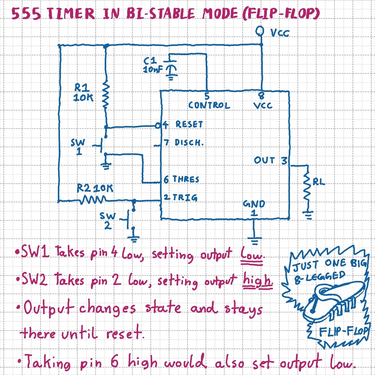
Bi-stable mode is arguably the least interesting way to use a 555 timer, as all it does Is expose the Internal flip-flop. I decided to talk about it first as it helps in understanding the basic behaviour of the chip and will make it easier to visualise what is happening inside the IC once we start adding external timing capacitors.
The job of this circuit is to toggle its output between HIGH or LOW (or ON or OFF), and hold it there until told to change state. You can think of it as a 1 bit memory module. Here’s how it works:
- R1 and R2 are pull-up resistors that keep pins 4 (Reset) and 2(Trig) high by default when the circuit is first powered on. Thus, the output at pin 3 is low.
- Pressing SW1 will ground pin 4(taking it low) but since output is already low, this would have no effect.
- Pressing SW2 will ground pin 2, causing the output to go high. Now pressing SW2 again will have no effect, until SW1 is pressed to take the output low again.
- Instead of the normally open switches, pins 4 and 2 can be controlled by some other digital circuit, such as a transistor switch controlled by the output of a microcontroller.
555 Timer in Monostable Mode
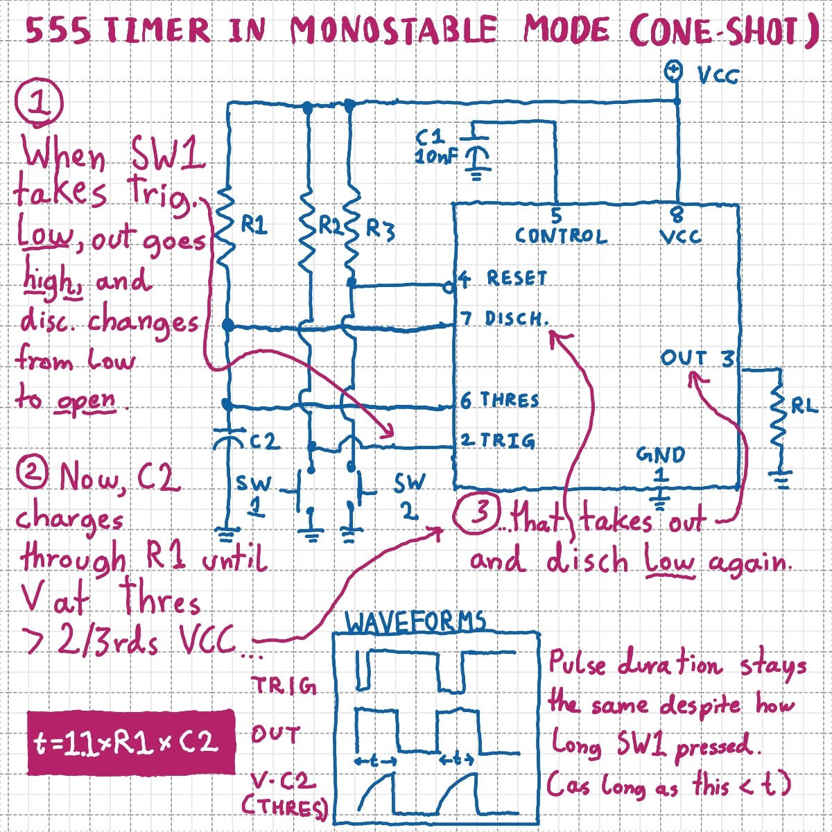
The 555 Timer’s monostable or one-shot mode of operation allows the generation of an output pulse of a precise duration. The duration of the output pulse is determined by a timing resistor and capacitor and is independent of the input or trigger pulse (As long as the trigger pulse is shorter than the output pulse).
As seen in Figure 5, pins 7 and 6 (Discharge and Threshold respectively) are tied together. This point in the circuit is also the junction of the RC network formed by R1 and C2. Pin 2 (Trigger) and pin 4 (Reset) are held high by 10K pull-up resistors R2 and R3 respectively. The circuit functions as follows:
1. Initially, pin 2 is at the same voltage as VCC. Since this is greater than 1/3rds VCC, the chip’s internal circuitry sets pins 3 (Output) and pin 7 (Discharge) at ground protentional. As a result of pin 7 being grounded, timing capacitor C2 cannot have a charge across it.
2. Forcing pin 2 low by a negative going pulse (closing SW 1 in the Figure 5 example) makes the internal flip-flop change state. This results in the output at pin 3 going high and pin 7 going open.
3. Since pin 7 is no longer shorting C2, the capacitor is now charging up towards VCC via R1. The rate at which the voltage across C2 climbs is determined by:
R1 ∗ C2The result is the time in seconds for the capacitor to charge to 0.606 VCC.
4. When C2 charges to over 2/3rds VCC, the comparator at pin 6 (Threshold) detects this and resets the internal flip-flop. This takes the output low again and grounds pin 7, discharging the capacitor. The output pulse has now ended, and the output stays low until the timer is triggered again.
555 Timer Monostable Mode Equation
The pulse time can be calculated by the following equation:
t = 1.1 R1 C2
Where R1 is the resistor connected to VCC, and C2 is the timing capacitor at pins 6 and 7.
555 Timer Monostable Mode Timing Chart
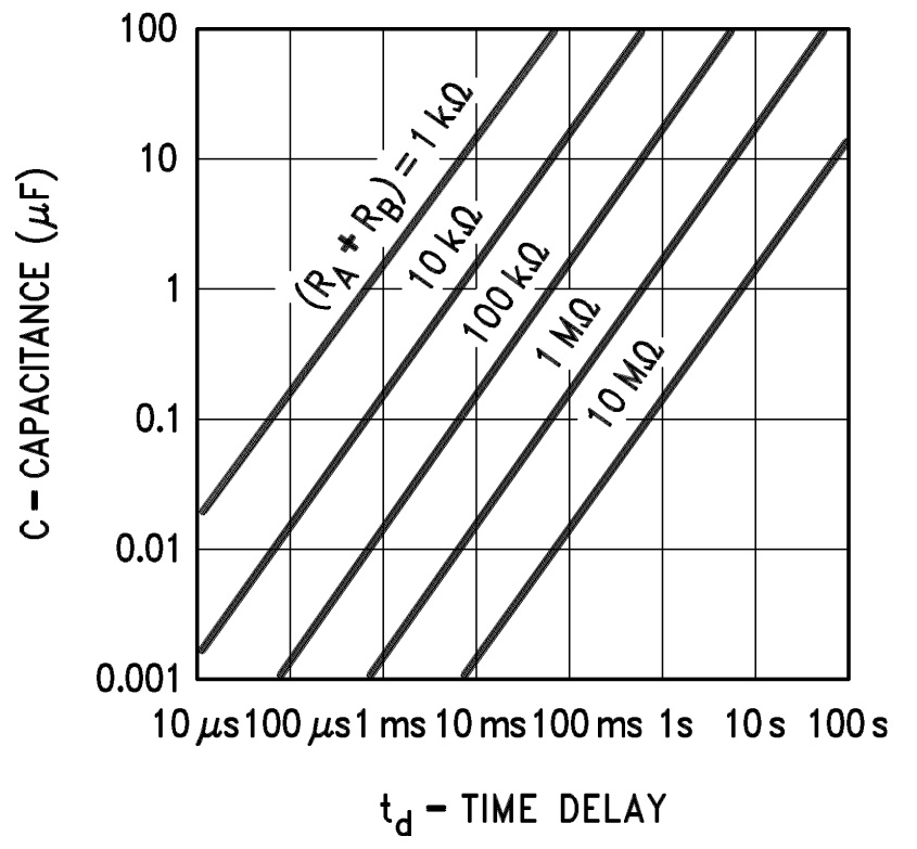
For your connivance a table showing various pulse durations for various combinations of R1 and C2 is shown below. You can also refer to the graph for monostable operation from the 555 Timer datasheet by Texas Instruments.
| 10K | 22K | 47K | 100K | 220K | 470K | 1M | |
| 1000uF | 11 | 24 | 52 | 110 | 240 | 520 | 1100 |
| 470uF | 5.2 | 11 | 24 | 52 | 110 | 240 | 520 |
| 220uF | 2.4 | 5.2 | 11 | 24 | 52 | 110 | 240 |
| 100uF | 1.1 | 2.4 | 5.2 | 11 | 24 | 52 | 110 |
| 47uF | 0.52 | 1.1 | 2.4 | 5.2 | 11 | 24 | 52 |
| 22uF | 0.24 | 0.52 | 1.1 | 2.4 | 5.2 | 11 | 24 |
| 10uF | 0.11 | 0.24 | 0.52 | 1.1 | 2.4 | 5.2 | 11 |
| 4.7uF | 0.052 | 0.11 | 0.24 | 0.52 | 1.1 | 2.4 | 5.2 |
| 2.2uF | 0.024 | 0.052 | 0.11 | 0.24 | 0.52 | 1.1 | 2.4 |
| 1.0uF | 0.011 | 0.024 | 0.052 | 0.11 | 0.24 | 0.52 | 1.1 |
| 0.47uF | 0.011 | 0.024 | 0.052 | 0.11 | 0.24 | 0.52 | |
| 0.22uF | 0.011 | 0.024 | 0.052 | 0.11 | 0.24 | ||
| 0.1uF | 0.011 | 0.024 | 0.052 | 0.11 | |||
| 0.047uF | 0.011 | 0.024 | 0.052 | ||||
| 0.022uF | 0.011 | 0.024 | |||||
| 0.01uF | 0.011 |
555 Timer Monostable Mode Tips
Here are some key points to keep in mind when designing 555 timer monostable mode circuits:
- Values of R1 below 1K should not be used.
- Avoid values below 10K as they will cause excess current flow and power consumption.
- Capacitor values over around 100uF will tend to produce inaccurate results due to capacitor leakage current.
555 Timer in Astable Mode
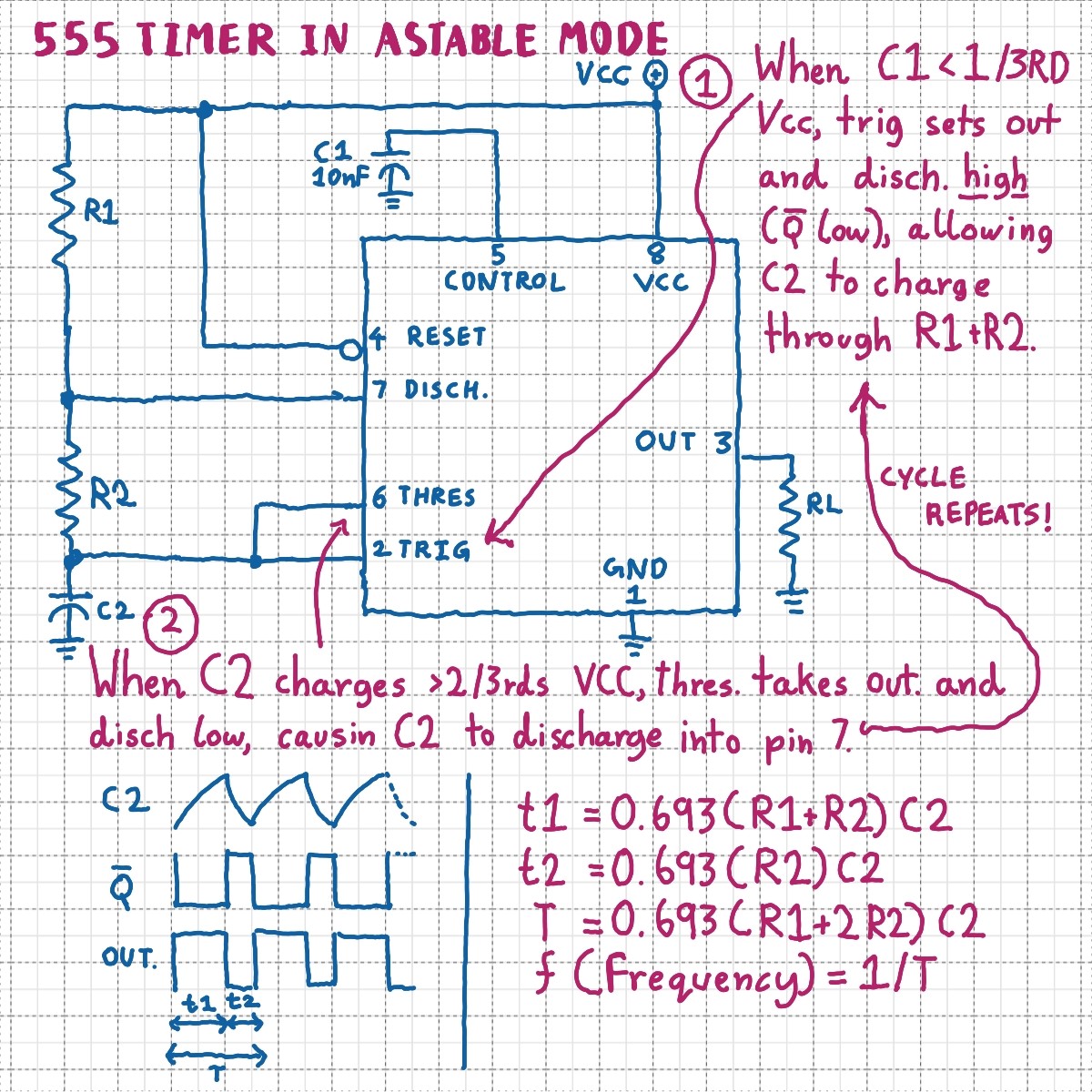
Astable mode turns the 555 Timer into a square wave oscillator that continuously generates an accurate pulse for as long as the circuit is powered on. Here’s how it works:
1. Referring to figure 7, when power is first applied C2 is discharged. Thus pin 2 is low. The chip detects this and sets the output high, and pin 7 open.
2. Since pin 7 is no longer grounded, C2 is able to start charging up through R1 and R2. When the voltage reaches 2/3rds of VCC, the chip detects this through pin 6 and sets output and pin 7 low again.
3. This causes C2 to start discharging into pin 7 through R2. When C2 discharges to under 1/3rds VCC, the chip detects this through pin 2 and the cycle repeats with the output going high and pin 7 going open again.
555 Timer Astable Mode Equations
The time in seconds for which the output is high is determined by:
t1 = 0.693 × (R1+R2) × C2The low time is determined by:
t2 = 0.693 × R2 × C2The total time of the cycle will be:
T = 0.693 × C2 × (R1 + 2 × R2)Thus the frequency will be:
f = 1.44 ÷ ((R1+ 2 × R2) × C2) = 1/T555 Timer Astable Mode Timing Chart
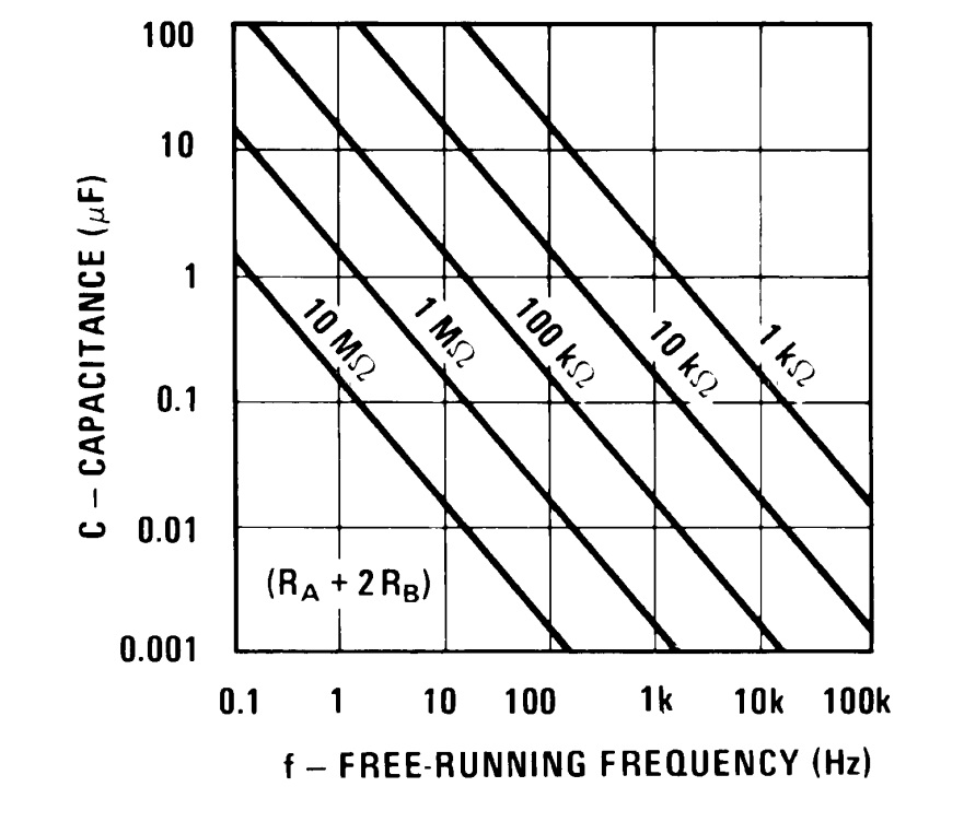
For your connivance a table showing the expected output frequency for various combinations of R1+R2 and C2 is presented below. You can also refer to the graph for monostable operation from the 555 Timer datasheet by Texas Instruments.
| R1 = 10K R2 = 10K | R1 = 10K R2 = 22K | R1 = 10K R2 = 47K | R1 = 10K R2 = 100K | R1 = 10K R2 = 220K | R1 = 10K R2 = 470K | R1 = 10K R2 = 1M | |
| 47uF | 1Hz | 0.57Hz | 0.3Hz | 0.15Hz | 0.068Hz | 0.032Hz | 0.015Hz |
| 22uF | 2.2Hz | 1.2hz | 0.63Hz | 0.31Hz | 0.15Hz | 0.069Hz | 0.033Hz |
| 10uF | 4.8Hz | 2.7Hz | 1.4Hz | 0.69Hz | 0.32Hz | 0.15Hz | 0.072Hz |
| 4.7uF | 10Hz | 5.7Hz | 3.0Hz | 1.5Hz | 0.68Hz | 0.32Hz | 0.15Hz |
| 2.2uF | 22Hz | 12Hz | 6.3Hz | 3.1Hz | 1.5Hz | 0.69Hz | 0.33Hz |
| 1.0uF | 48Hz | 27Hz | 14Hz | 6.9Hz | 3.2Hz | 1.5Hz | 0.72Hz |
| 0.47uF | 100Hz | 57Hz | 30Hz | 15Hz | 6.8Hz | 3.2Hz | 1.5Hz |
| 0.22uF | 220Hz | 120Hz | 63Hz | 31Hz | 15Hz | 6.9Hz | 3.3Hz |
| 0.1uF | 480Hz | 270Hz | 140Hz | 69Hz | 32Hz | 15Hz | 7.2Hz |
| 0.047uF | 1kHz | 570Hz | 300Hz | 150Hz | 68Hz | 32Hz | 15Hz |
| 0.022uF | 2.2kHz | 1.2kHz | 630Hz | 310Hz | 150Hz | 69Hz | 33Hz |
| 0.01uF | 4.8kHz | 2.7kHz | 1.4kHz | 690Hz | 320Hz | 150Hz | 72Hz |
| 4700pF | 10kHz | 5.7kHz | 3kHz | 1.5kHz | 680Hz | 320Hz | 150Hz |
| 2200pF | 22kHz | 12kHz | 6.3kHz | 3.1kHz | 1.5kHz | 690Hz | 330Hz |
| 1000pF | 48kHz | 27kHz | 14kHz | 6.9kHz | 3.2kHz | 1.5kHz | 720Hz |
| 470pF | 100kHz | 57kHz | 30kHz | 15kHz | 6.8kHz | 3.2kHz | 1.5kHz |
| 220pF | 220kHz | 120kHz | 63kHz | 31kHz | 15kHz | 6.9kHz | 3.3kHz |
| 100pF | 480kHz | 270kHz | 140kHz | 69kHz | 32kHz | 15kHz | 7.2kHz |
Independent Adjustment of On Time and Off Time in Astable Mode
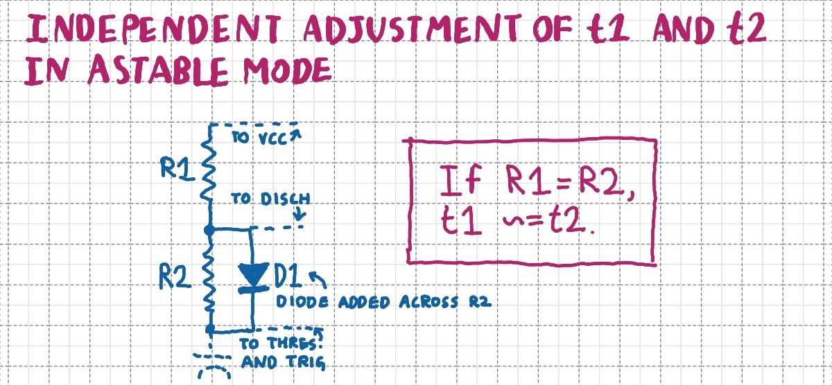
Since the capacitor charges through R1 and R2, but discharges only through R2, the on and off time cannot be equal or adjusted independently. A workaround is to connect a diode across R2 as shown in figure 9. This will allow R1 to only determine the on time while R2 only determines the off time.
Using the 555 Timer Output
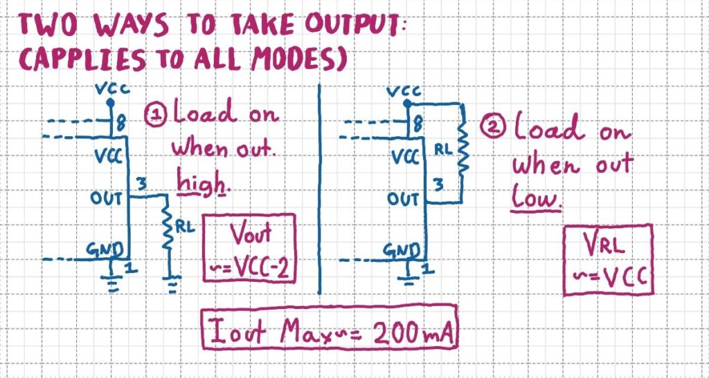
In the examples above, the “load” was shown connected between pin 3 and ground as resistor RL. In practical applications RL will be replaced by whatever circuit or component you wish to power when the timer is high. The output voltage will be around VCC-2, and the maximum current that the 555 timer is capable of sinking through the output is around 200mA. (Refer to the datasheet for the exact version of the chip that you are using.)
Chaining 555 Timers

Figure 11 illustrates four ways in which one 555 Timer can be used to control another. In theory, as many timers may be chained together as needed using these methods, which are summed up below:
- Connecting timer 1’s output (pin 3) to timer 2’s VCC (pic 8) will cause timer 2 to run only while timer 1’s output is high.
- Connecting timer 1’s output to timer 2’s trigger (pin 2) will trigger timer 2 when timer 1’s output goes high.
- Connecting timer 1’s output to timer 2’s control (pin 5) will cause timer 2’s threshold voltage to change according to timer 1’s output. This results in frequency modulation of timer 2’s output when it is operating in astable mode.
- Timer 1’s output connected to timer 2’s reset (pin 4) will force timer 2 to reset whenever timer 1 goes low. This can be used to “sync” timer 2 to timer 1.
555 Timer Applications
Armed with an intuitive understanding of the 555 timer’s functioning, you can now no doubt imagine your own creative applications for this iconic chip. Electronics hobbyist have found numerous unusual ways to use the 555, such as this 555 Timer based radio receiver. To complete this article however, I have presented three “typical” uses of the chip for representative purpose.
555 Timer Time-Delay Relay Driver Circuit
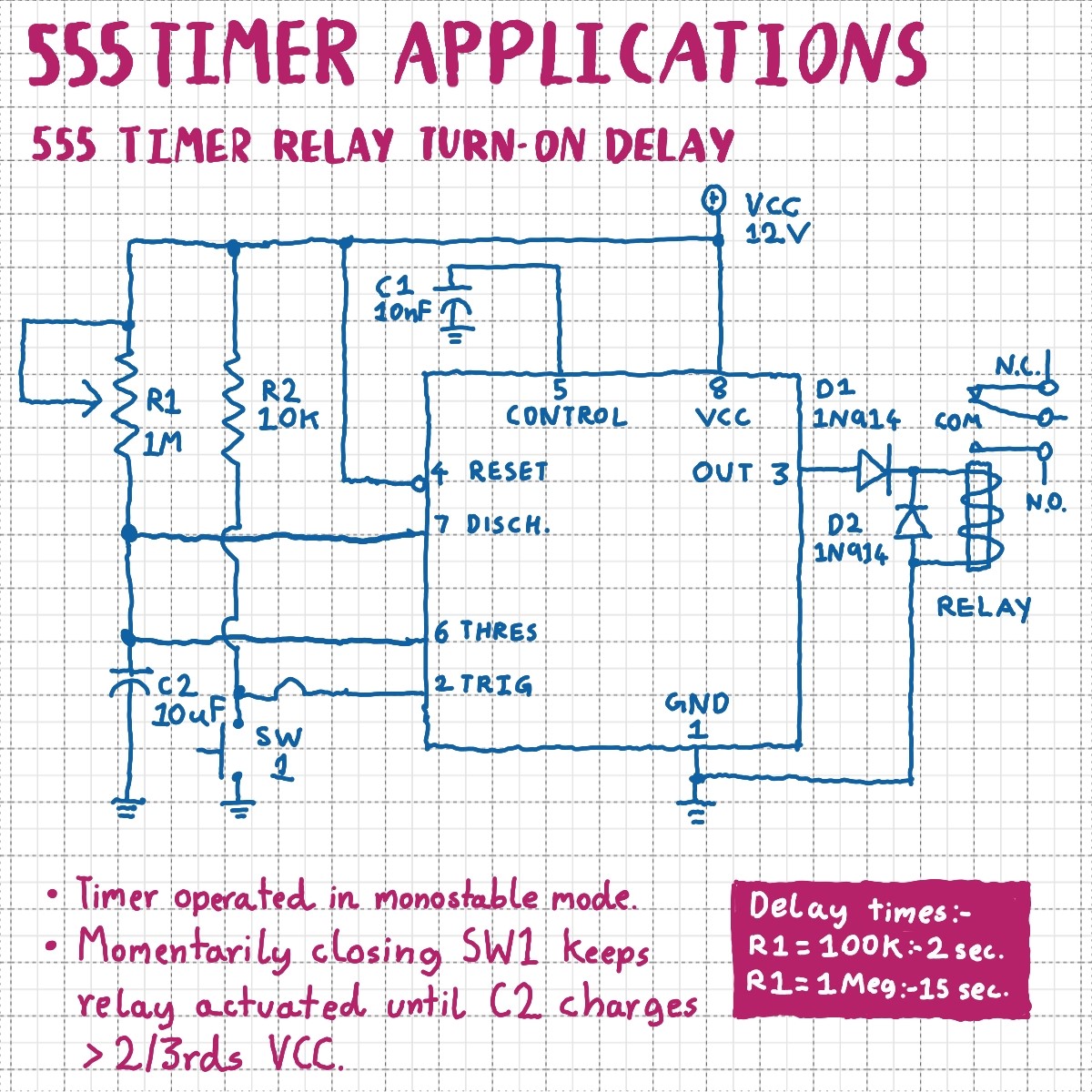
In many cases, it is desirable for a circuit to be powered on after a short delay. In the above circuit, SW1 is to be closed as the circuit is powered on (maybe the SW1 contacts could be part of the device’s main power switch, or a negative pulse to the trigger pin from a microcontroller could be used as well). This causes the output to go high, actuating the relay. If the normally closed (N.C.) and common (COM) contacts of the relay are in series with the power supply to the secondary circuit, the timer will hold the secondary circuit off until C2 charges to over 2/3rds VCC. D1 and D2 protect the IC from voltage spikes caused by the relay’s inductance. Since this is essentially a monostable circuit, the same equation can be used to get an approximation of the delay time:
t = 1.1 R1 C2You can expect around 2 seconds of delay with R1 = 100K and C2 = 10uF. This rises to 15 seconds if R1 is set to 1 Meg.
Basic Tone Generator or Metronome with 555 Timer
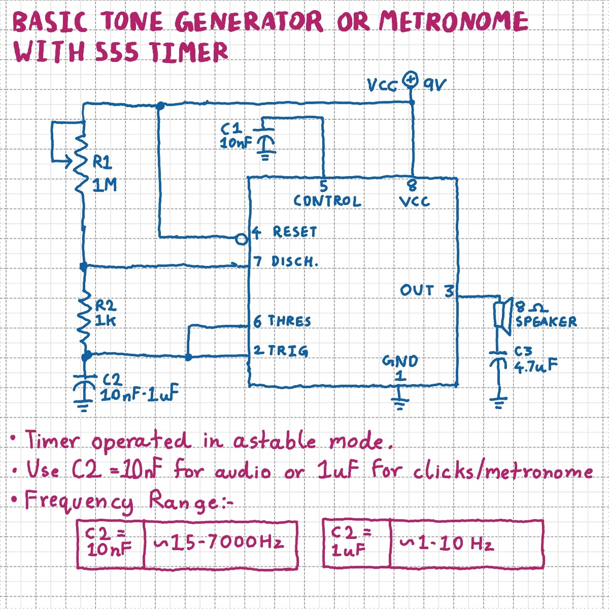
Generating audible tones is one of the most common applications of the 555 timer. In the above example, the 555 timer is operated in astable mode, hence the output frequency will be approximately:
f = 1.44 ÷ ((R1 + 2 × R2) × C1)Using a potentiometer connected as a variable resistor for R1 allows you to adjust the frequency on the fly. With R1 = 1Meg, R2 = 1K use C2 = 10nF for an audio frequency output between around 15Hz to 7kHz. With C2 = 1uF, the circuit can act as a metronome or click generator by operating between around 1-10Hz.
555 Timer Dual LED Flasher Circuit
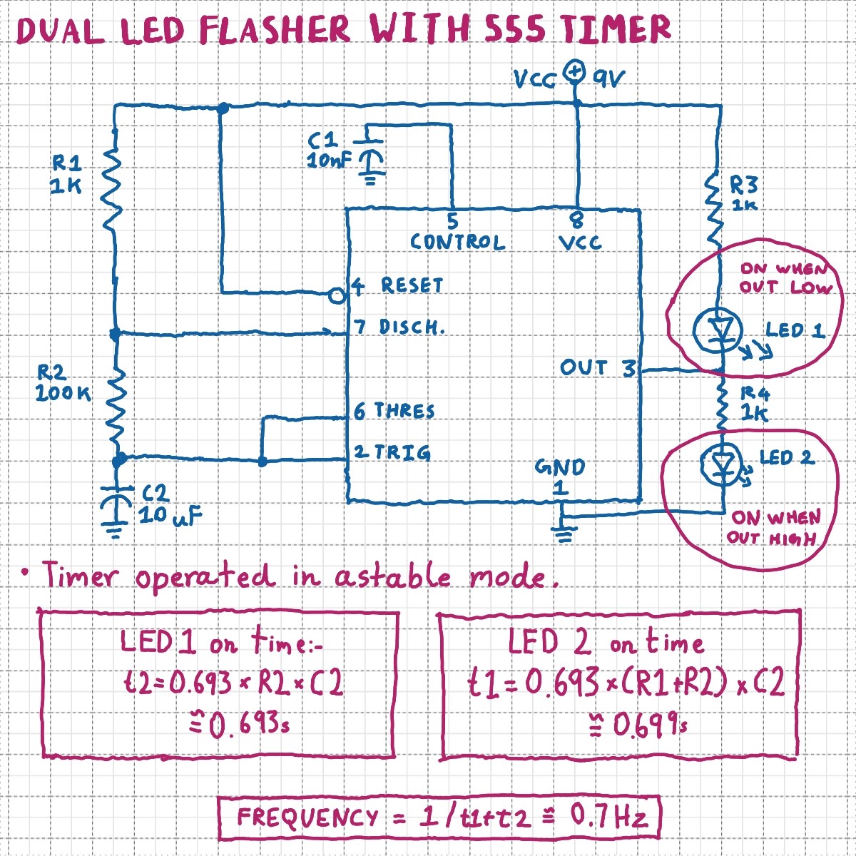
Another very common use of the 555 timer is to flash LEDs. The above circuit turns each LED on and off one after the other. Note that LED1’s cathode is connected to the output, thus it turns on when the output is low. On the other hand, LED2’s anode is connected to the output (via R4), thus it turns on when the output is high. Since this is simple astable mode operation of the 555 timer, the same equations can be used to calculate the on and off times of each LED and the frequency of flashes.
t1 = 0.693 × (R1+R2) × C2 ~= 0.699s
t2 = 0.693 × R2 × C2 ~= 0.693s
T = 0.693 × C2 × (R1 + 2 × R2) = t1+t2 ~= 1.392s
f = 1.44 ÷ ((R1+ 2 × R2) × C2) = 1/T ~= 0.7Hz
Where t1 is LED 2’s on-time and t2 is LED 1’s on time.
555 Timer Stepped Tone Generator / Atari Punk Console Circuit

This is an extremely popular circuit by the legendary Forrest M. Mimms III. A favourite of DIY synthesizer and electronic music hobbyists, the circuit is popularly called “Atari Punk Console” for the retro video-game console like sounds it generates. Forrest Mimms presented the circuit using a 556 dual timer, but I have shown it here using two separate 555s to make its operation clearer. Essentially, the first timer is operated in astable mode, while the second timer is operated in monostable mode. This mean that timer 1 is generating a constant free-running oscillation while timer two only generates a pulse when triggered. Since timer 2 is triggered by timer 1, adjusting timer 2’s pulse width using R3 makes the output pitch appear to change in “steps” instead of a smooth graduation. This is because the output pulses are forced to “align” to the “grid” generated by the first timer.
555 Timer “Siren” Generator
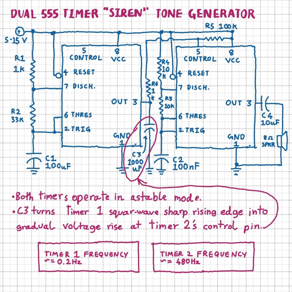
The circuit above uses two 555 timers (or one 556 dual timer) to create a “police siren” like sound that smoothly changes pitch on its own. Both timers are operated in astable mode, with the first timer’s output feeding the second timer’s input via current limiting resistor R6. Note the very large 1000uF capacitor, C3, connected to timer 1’s output. Since this capacitor takes a while to charge, timer 1’s abrupt rising edges are smoothed out into a gradually rising voltage. This smoothened out voltage change applied to timer 2’s control pin causes a “smooth” change in timer 2’s output frequency. Note that timer 1’s timing capacitor C1 is a much larger value than timer 2’s timing capacitor C2. Timer 1 thus acts as a low-frequency-oscillator that frequency modulates the timer 2.
The usual astable mode equations can be used to calculate the output frequencies:
fTimer1 = 1.44 ÷ ((R1+ 2 × R2) × C2) = 1/T ~= 0.2Hz
fTimer 2 = 2 f = 1.44 ÷ ((R1+ 2 × R2) × C2) = 1/T ~= 480Hz
OK, but What ACTUALLY is Inside The 555 Timer?
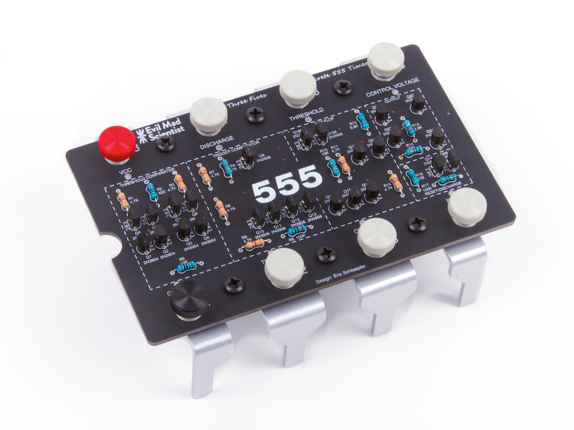
Encased inside the black plastic casing is a thin wafer of silicon, areas of which have been “doped” with impurities to form transistors, diodes, and resistors. The working of semi-conductors and IC fabrication go way beyond the scope of this article, but if you do wish to understand the 555 Timer on a transistor-level I recommended checking out the “Three Fives” Discrete 555 Timer kit from Evil Mad Scientist Laboratories. Check out the kit’s accompanying instructions for a transistor-level description of the 555’s internal circuit.
More 555 Timer Circuits and Information
The 555 timer will certainly appear on this blog again, especially in the context of sound synthesis circuits. If you interested in 555 timer and other old school IC and transistor based analog audio circuits, be sure follow @_electroidiot on Instagram and subscribe to the _electroidiot mailing list below to stay updated! Also check-out the suggested reading material at the end of this post for some essential resources and reading on the 555 timers.
Get Notified of New Posts, subscribe to the _electroidiot Mailing List.
Recommended Reading
One of the best explanations about the 555 timer’s functioning that I’ve found is by Charles Platt in his book “Make: Electronics”. I highly recommend you pick up a copy of this book, especially if you enjoy a hands-on project-based approach to learning Electronics.

Make: Electronics: Learning by Discovery: A hands-on primer for the new electronics enthusiast
Check out following resources to learn more about the 555 Timer:
- Make: Electronics by Charles Platt.
- 555 Timer Applications Sourcebook by Howard M. Berlin.
- 555 Timer IC Circuits (Engineer’s Mini-Notebook) by Forrest M. Mimms III
- Getting Started in Electronics by Forrest M. Mimms III
- “Getting to know the 555” article on Adafruit.


Leave a Reply